Schematics
Here you can find more information about the different components that are included on the schematic. These are symbols that represent the inputs and outputs of the electrical components that make the board work.
Download a PDF of the Schematics
The schematics are broken down into the following parts:
- WiFi Module
- Power Supply
- Display
- User Input
- Programming
WiFi Module
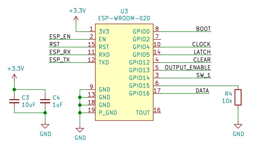 The ESP WROOM 02 acts as the microcontroller for this design. It is a module that includes both the ESP8266 and a WiFi antenna that is made using a trace on the module’s circuit board. This means that we get all the parts needed to make the microcontroller and WiFi work on one simple module. We only have to worry about a few power filtering capacitors and a pull down resistor on pin 6, GPIO 15. This pull down resistor is used for making sure the WiFi module doesn’t try and boot from an SD card on startup.
Want a deep dive into how this module works and what’s needed to add one to your design?
Check out the datasheet from Espressif
Inputs and Outputs
There are a few inputs and outputs that we need to worry about to get all the lights blinking in just the right way.
UART
This is the communication protocol used to program the module and read any debug information as it is running.
| Name | Direction | Description |
|---|---|---|
| ESP_RX | input | Serial Communication going to the WiFi module |
| ESP_TX | output | Serial Communication coming from the WiFi module |
These signals will be routed to the programming header J2.
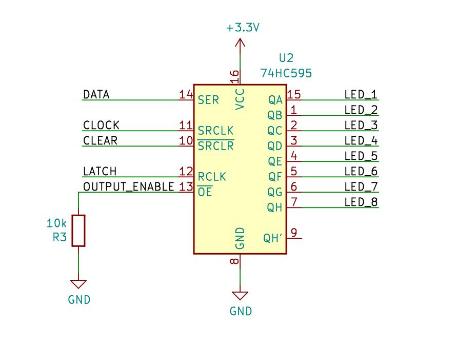
Shift Register
In order to put data from the WiFi module (a packet of 8 bits, corresponding to which LED to turn on) we need to attach some GPIO signals between the WiFi module and the shift register U2.
| Name | Direction | Description |
|---|---|---|
| CLOCK | output | clock input for all d flip-flops |
| LATCH | output | causes whatever data is in the shift register to appear on the output |
| CLEAR | output | clears whatever data is in the shift register (sets to 0), active low |
| OUTPUT_ENABLE | output | allows output to be either 1 or 0, if disabled they will become high impedance, active low |
| DATA | output | serial data input stream, this is what gets ‘clocked’ in |
Active Low or Active High?
Most digital signals are “Active High”, the circuit sees a digital 1 when the voltage is at or near the supply voltage (here it’s 3.3 V).
“Active Low” signals are the opposite, and require a low voltage (at or near 0 V) to indicate a logical 1 or to do something. For us, the CLEAR and OUTPUT_ENABLE signals are Active Low. Therefore we will set them to 0 V when we want them to do the thing their name implies.
Chips will use Active Low signals to help reduce the chance of errors resulting from electrical noise. When we are applying a voltage above ground, noise from all sorts of sources can cause that voltage to swing, possibly below the threshold for what the IC sees as “high”.
When signals have a clear path to ground (or are directly connected to ground), it is a lot harder for noise to appear, since any voltage will quickly dissipate.
learn more about how logic levels work
Power Supply
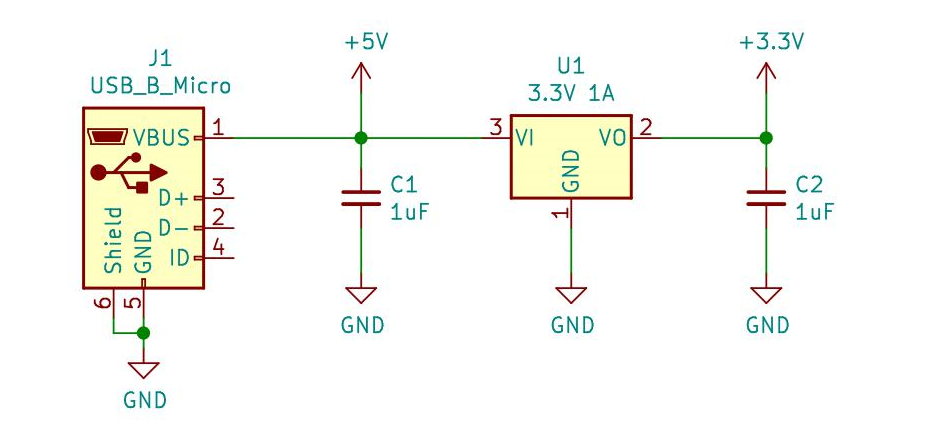
This part of the circuit is what takes the input voltage from the USB connector (or the programming header) and regulating the voltage down to 3.3 Volts for the rest of the components. It is a smiple Low Dropout Linear Regulator (LDO). This means that it will “burn off” extra voltage on the input and create the voltage we want on the output. One downside to these types of regulators is that they can waste some energy, which turns to heat coming out of the part.
We can assume the USB port has a voltage of around 5 V, but what if someone gives the board another voltage?
The voltage regulator (Diodes Incorporated AZ1117CH-3.3TRG1) has a rated max input voltage of 15 Volts, and voltage dropout of 1.3 Volts at 800 mA. This means the board can safely accept a voltage of between 4.6 and 15 Volts. If the input voltage starts dropping below 4.6 V, then the output voltage will also start to drop, which can affect the performance of the rest of the circuit.
Learn more about LDO regulators specifications
Display
Here is the circuit that takes the data coming from the microcontroller and outputs that data on the 8 LEDs.
Shift Register
Why do we even need this?
Good question! Often times we need to ask ourselves this, to be able to justify our design decisions so that we don’t assume we’re making the right decision and so we know we are making the right one.
An alternative to using this extra IC is to just simply hook up the 8 LEDs directly to GPIO on the WiFi module. In order to do this however, we would take up a lot of ports and have to use some that are needed for programming.
Using a shift register allows us to use less GPIO ports, and even allows the design to expand past 8 LEDs without needing extra signals coming from the WiFi Module. At the cost of extra parts, we gain simplicity and a chance to learn about how to use a nifty part!
Maybe you could make do without it?
Want a chance to reduce how many parts are in the circuit (and therefore cost)? See if you can redesign the circuit to do away with the shift register!
How does it work?
The 74HC595 is an example of a “Serial Input, Parallel Output” shift register, since it takes data in one bit at a time, and can output all the bits of the stored data at once. Every time the CLOCK signal transitions from low to high, it places whatever was on the DATA pin (either 1 or 0) into storage. This storage starts at Q0, and every time a new bit is “clocked in” the value of Q0 moves to Q1, and Q0 becomes the value of DATA.
When the next time a bit is clocked in, the value of Q1 is moved to Q2, Q1 becomes the value of Q0, and Q0 becomes the value of DATA. All the way until Q7 becomes the value of Q6, and the first bit we clocked in is all the way at Q7.
When all 8 bits have been loaded into the shift register, it is time to display them. This is done with a transition from low to high on the LATCH pin.
If we latched every time we clocked in a new bit, we would see each intermediate step as the 8 bits are loaded in. Since we want to make sure only the right LEDs are on, we wait until everything is ready to latch the data to the output.
To allow us to control the brightness, we can use the OUTPUT_ENABLE pin as a final “light switch” that we can turn on and off really quickly to make the apparent brightness lower.
If this is your first time learning about shift registers, check out this turorial from Arduino.
For a more detailed description of this IC, be sure to have a look at the datasheet.
LEDs
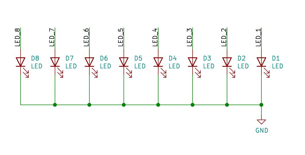
Each output of the shift register (Q0-Q7, eight in total), is connected directly to the anode (+) of an LED. Normally, we would need to add a current limiting resistor when using an LED. Here we don’t have one, why is that?
LED Forward Voltage
LEDs operate with a “non-linear” IV curve. This means that the device will not adhere to the V = IR that resistors follow. The LED will turn on, and start drawing significantly more current. The voltage at which this happens is known as the Forward Voltage.
From the datasheet of the Lite-On LTST-C150TBKT LEDs, we can find the IV curve, and estimate what the current would be at 3.3 Volts.
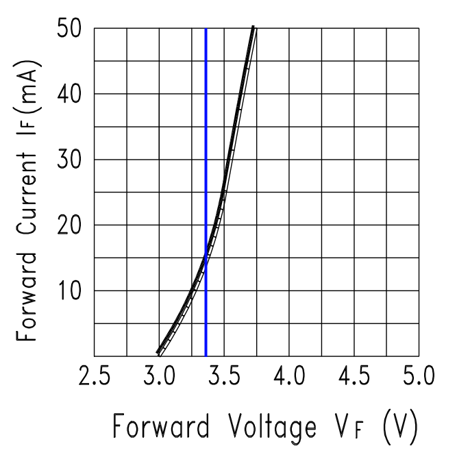
From this curve, we can estimate that each LED will draw 15 mA of current when the shift register is outputting a logic 1, which will be 3.3 Volts.
Current Sink, or Source?
In its current orientation, the circuit works in a current source configuration. This means that current will flow out of the shift register and then through the LEDs.
Another way to light LEDs would be to sink the current, which would mean the current is coming from the voltage regulator through the LEDs and then through the shift register to ground. This would mean having the anode of the LEDs connected to the 3.3 V supply, and the cathodes connected to the shift register outputs. In current sink configuration, when the shift register outputs a 0, the current is allowed to flow and the LED turns on.
Checking the datasheet for the 74HC595 Shift Register, we see that the supply current is rated for a maximum of 70 mA for each output pin.
This means we can use the shift register in a current source configuration without worrying about drawing too much current from the shift register, since an LED will only draw 15 mA at 3.3 Volts.
User Input
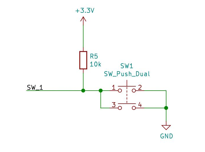
In order to let the user interact with the circuit, a simple switch is added with a pull up resistor. When the button is pressed, current is allowed to flow through the resistor and the microcontroller reads a digital 0 as SW_1 is connected to GND.
Programming
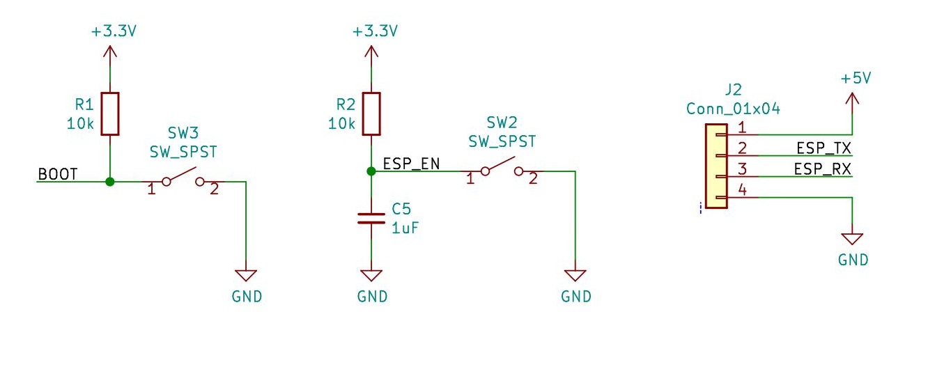
The way that new code is flashed onto the ESP-WROOM-02 Module is through the UART ports, which are routed to the PCB header.
The two buttons are added to make it easier to put the WiFi module into programming mode.
In order to do so, GPIO 0 on the module must be low when the module powers on, and ESP_EN resets the board when pulled low, and will power on when back high.
To Enter Programming Mode
hold down both BOOT and EN buttons, and then let go of EN before releasing BOOT